
Σ-Δ轉換器使用從調節器得到的許多采樣值產生1bit碼流。Σ-ΔADC以高采樣速率使用輸入信號量化器完成這個任務。像所有的量化器一樣,Σ-ΔADC調節器獲取輸入,產生數字碼流表征輸入電壓。可以觀察時域或頻域的Σ-Δ調節器。如果看時域表現,可以見一階調節器的結構(圖1)。
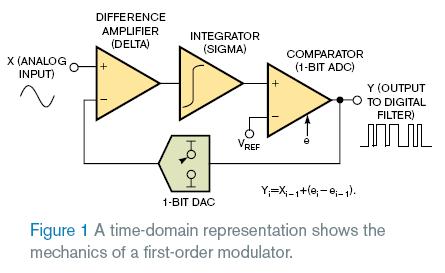
調節器測量模擬輸入信號和反饋DAC的模擬輸出。隨后一個積分器測量求和節點的模擬電壓輸出,為1位ADC呈現出一個斜坡信號。1位ADC轉換積分器輸出信號為數字一或零。使用系統時鐘,ADC將1位數字信號送到調節器輸出,也通過反饋回輸入,在這里1位DAC為等待。
1位ADC將信號量化為離散的輸出編碼,帶有轉換器的量化噪聲(ei)。調節器輸出等于輸入信號加上量化噪聲(ei–ei–1)。如這個公式所示,量化噪聲為調節器當前誤差(ei)減去前一個誤差(ei–1)的微分。時域輸出信號為以采樣頻率FS的輸入信號脈沖波形。如果將輸出脈沖序列平均,它等于輸入的信號值。
頻域圖反映了不同的問題(圖2)。時域輸出脈沖在頻域內表現為輸入信號(或毛刺)和變形的噪聲。圖2的噪聲特性是調節器頻率作用的關鍵。

不像大
多數量化器,Σ-Δ調節器包括形成量化噪聲的積分器。調節器輸出的噪聲頻譜并不平滑。更重要的,在頻率分析中,可以看到積分器怎樣在更高頻率處形成噪聲,便于產生更高分辨率的結果。
圖2中調節器輸出顯示了調節器的量化噪聲在0Hz時開始為低電平,快速上升,然后在調節器采樣頻率為最大值處穩定。
二階調節器進行兩次積分,而不是僅有一次,是最小化低頻率量化噪聲的一種好方法。大多數Σ-Δ調節器具有更高的階數。例如,更常用的Σ-Δ轉換器的設計包括二、三、四、五或六階調節器。多階調節器在更高頻率形成更大的量化噪聲。
英文原文:
Delta-sigma ADCs in a nutshell, part 2: the modulator
Unlike most quantizers, the delta-sigma modulator includes an integrator that shapes the quantization noise.
By Bonnie Baker -- EDN, 1/17/2008
A delta-sigma converter uses many samples from the modulator to produce a stream of 1-bit codes. The delta-sigma ADC accomplishes this task by using an input-signal quantizer running at a high sample rate. Like all quantizers, the delta-sigma modulator takes an input and produces a stream of digital values that represents the voltage of the input. You can look at the delta-sigma modulator in the time or in the frequency domain. If you look at a time-domain representation, you can see the mechanics of a first-order modulator (Figure 1).
The modulator measures the difference between the analog-input signal and the analog output of a feedback DAC. An integrator then measures the analog-voltage output of the summing junction and presents a sloping signal to the 1-bit ADC. The 1-bit ADC converts the integrator’s output signal to a digital one or zero. Using the system clock, the ADC sends the 1-bit digital signal to the modulator’s output, as well as back through the feedback loop, where a 1-bit DAC is waiting.
The 1-bit ADC digitizes the signal to a coarse output code that has the quantization noise (ei) of the converter. The modulator output is equal to the input plus the quantization noise, (ei–ei–1). As this formula shows, the quantization noise is the difference of the current error (ei) minus the previous error (ei–1) of the modulator. The time-domain output signal is a pulse-wave representation of the input signal at the sampling frequency, fS. If you average the output-pulse train, it equals t
he value of the input signal.
The frequency-domain diagram tells a different story (Figure 2). The time-domain output pulses in the frequency domain appear as the input signal (or spur) and shaped noise. The noise characteristic in Figure 2 is the key to the modulator’s frequency operation.
Unlike most quantizers, the delta-sigma modulator includes an integrator that shapes the quantization noise. The noise spectrum at the modulator output is not flat. More important, in a frequency analysis, you can see how the modulator shapes the noise to higher frequencies, facilitating the production of a higher resolution result.
The modulator output in Figure 2 shows that the quantization noise of the modulator starts low at 0 Hz, rises rapidly, and then levels off at a maximum value at the modulator sampling frequency.
Integrating twice with a second-order modulator, instead of just once, is a great way to minimize low-frequency quantization noise. Most delta-sigma modulators are of a higher order. For instance, the designs of the more popular delta-sigma converters include second-, third-, fourth-, fifth, or sixth-order modulators. Multi-order modulators shape the quantization noise even harder to higher frequencies.
References
Baker, Bonnie, “Delta-sigma ADCs in a nutshell,” EDN, Dec 14, 2007, pg 22.
Baker, RJ, CMOS mixed-signal circuit design, Wiley & Sons, ISBN 0471227544, May 2002.